semiconductor wafer 6inch prime sillicon wafer, sillicon optical lens, IC sillicon substrates , poly sillicon wafer,Semiconductor 3' inch silicon wafer, single crystal ,2inch, 3inch,4inch,5inch,6inch,8inch,12inch silicon wafer, single side polished silicon wafer, customized si lens ,sillicon lens
1. Description
|
Density | 2.4(g/cm3) | | |
| Dope type | no dope | doped B | doped P |
| Type | I | P | N |
| resistivity | Ø 1000Ωcm | 10-3~40Ωcm | 10-3~40Ωcm |
| E P D | ≤100∕cm2 | ≤100∕cm2 | ≤100∕cm2 |
| Oxygen content (∕cm3) | ≤1~1.8×10¹⁸ | ≤1~1.8×10¹⁸ | ≤1~1.8×10¹⁸ |
| Carbon content(∕cm3) | ≤5×10¹⁶ | ≤5×10¹⁶ | ≤5×10¹⁶ |
| Size | 10×3m,10×5m,10×10mm,15×15mm, | | |
| Dia5-100mm | | |
| or by customized size | | |
| thickness | 0.5mm,1.0mm or other | | |
| tolerance | <±0.1mm | | |
| thickness tolerance | <±0.015mm (or <±0.005mm) | | |
| surface | 1sp or 2sp | | |
| orientation | ±0.5° | | |
| | | | |
| orientation | <100>,<110>,<111> | | |
| package | 100grade in1000 grade cleaning room | | |
Supply kinds of Plano convex Si-lens, Bi-convex Si-lens, Plano concave Si-lens, Bi-concave
Si-lens (Infrared Silicon Lenses).
Silicon (Si) is grown by Czochralski (CZ) pulling techniques. CZ Silicon is commonly used as substrate material for infrared reflectors and windows in the 1.5 - 8 micron region. The strong absorption band at 9 microns makes it unsuitable for CO2 laser transmission applications, but it is frequently used for laser mirrors because of its high thermal conductivity and low density. Applications: window, lens in the
1.5 - 8 m region and mirrors for CO2 laser and spectrometer applications
Si Len Specifications:
Material: Silicon
Diameter Tolerance: +0.00, -0.15mm(Standard), +0.00,-0.02mm(Precision)
Flatness: lambda 632.8nm
Surface Quality: 60-40 S/D
Paraxial Focus Length: +/-2%
Centration: <10arc minutes
Clear Aperture: >85% of diameter
Bevel: 0.25x45de
2. sample: dia25x3mmt si lens


3 About our company
SHANGHAI FAMOUS TRADE CO.,LTD. locates in the city of Shanghai, Which is the best city of China,
and our factory is founded in Wuxi city in 2014.
We specialize in processing a varity of materials into wafers, substrates and custiomized optical glass parts.components widely used in electronics, optics, optoelectronics and many other fields. We also have been working closely with many domestic and oversea universities, research institutions and companies, provide customized products and services for their R&D projects.
It's our vision to maintaining a good relationship of cooperation with our all customers by our good reputatiaon.
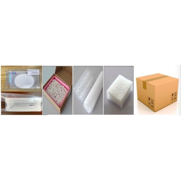
4. packing and delivery
---FAQ –
Q: Are you trading company or manufacturer ?
A: zmkj is a trading company but have a sapphire manufacturer and,
as a supplier of semiconductor materials wafers for a wide span of applications.
Q: How long is your delivery time?
A: Generally it is 5-10 days if the goods are in stock. or it is 15-20 days if the goods are not
in stock,it is according to quantity.
Q: Do you provide samples ? is it free or extra ?
A: Yes, we could offer the sample for free charge but do not pay the cost of freight.
Q: What is your terms of payment ?
A: Payment<=1000USD, 100% in advance. Payment>=1000USD,
50% T/T in advance ,balance before shippment.
If you have another question, pls feel free to contact us as below:
Product Tags:

|
|
Double Side Polished IC Silicon Wafer Customized Si Lens For Optical Lens Images
|


